

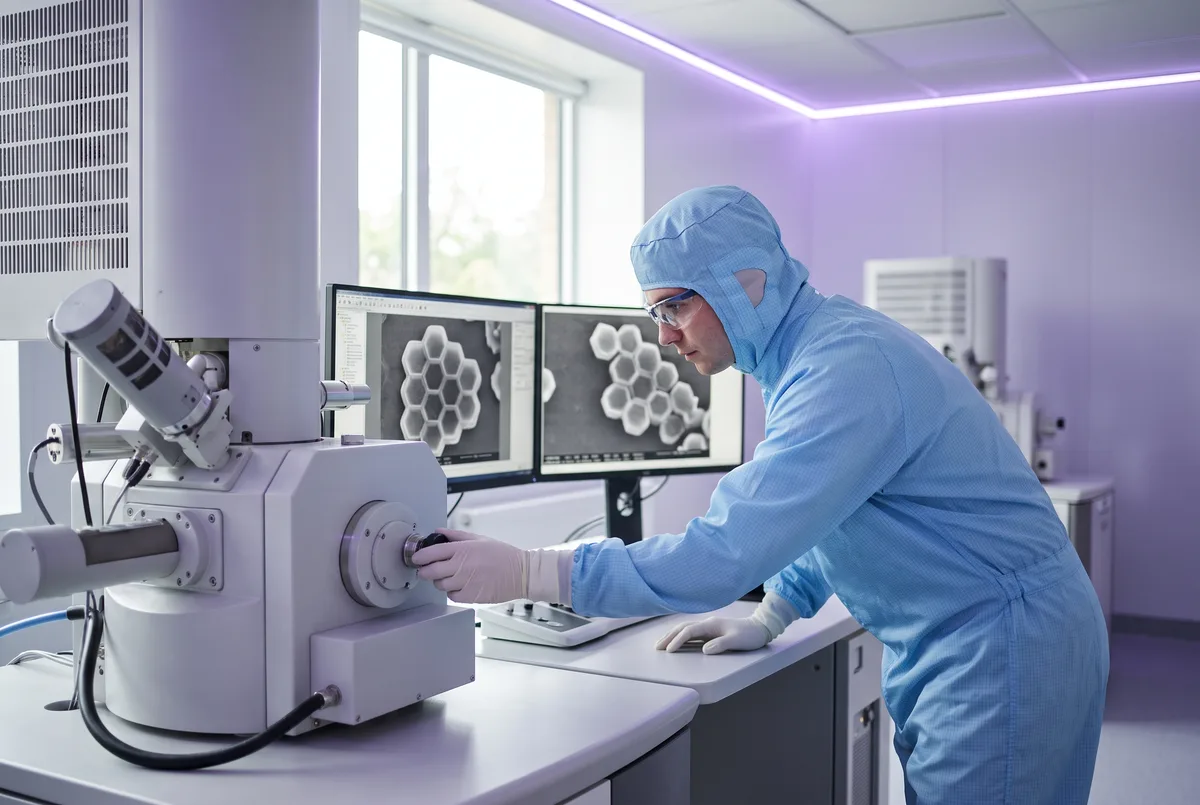
Surface morphology study by SEM
Price on requestScanning electron microscopy: surface and fracture imaging, feature size assessment; low-vacuum mode allows non-conductive samples without sputter coating.
Al-Farabi KazNU · open-access laboratory
Nanomaterials and nanoelectronics: graphene, carbon nanotubes, thin films. An open-access laboratory that, per public sources, explicitly offers services to external clients. Its instrument park is set up for third-party samples.
This catalogue is informational: it was compiled by the hub from open sources and is not an offer. The hub does not act as a representative of the university and does not dispose of its equipment. Scope, timelines and prices are confirmed by the laboratory for every request.
An open-access laboratory at KazNU. Core topics: synthesis and diagnostics of nanomaterials (graphene, carbon nanotubes), nanoelectronics and thin-film coatings. Available methods include electron and atomic-force microscopy, Raman spectroscopy (including tip-enhanced), X-ray scattering and diffraction, optical spectrophotometry and vacuum thin-film deposition. Service scope, instrument availability and pricing are to be confirmed with the lab.
This list was compiled by the hub from open data and is subject to confirmation by the laboratory.
Scanning electron microscopy: surface and fracture imaging, feature size assessment; low-vacuum mode allows non-conductive samples without sputter coating.
Surface topography and profilometry at nanometre resolution, roughness and film-thickness assessment.
Raman spectra, including tip-enhanced (TERS): identification of carbon materials, defect density and graphene layer count.
Nanoparticle size, porosity and supramolecular structure; phase analysis of crystalline materials.
Vacuum deposition of thin-film coatings onto client substrates with thickness control.
| Instrument | Model | Used for | Category |
|---|---|---|---|
| Scanning electron microscope (SEM) | Quanta 200i 3D | Surface and fracture morphology, microstructure analysis, non-conductive samples. | Microscopy |
| Scanning probe microscope (AFM) | Integra | Nanometre topography, roughness, film thickness. | Microscopy |
| AFM–Raman system (TERS) | — | Co-located topography and chemical identification; tip-enhanced signal. | Spectroscopy & mass spectrometry |
| X-ray scattering system | SAXS/WAXS | Nanoparticle size, porosity, supramolecular structure of polymers and composites. | Spectroscopy & mass spectrometry |
| X-ray diffractometer | Rigaku MiniFlex 600 | Phase analysis of powders and coatings, crystallite size estimation. | Spectroscopy & mass spectrometry |
| UV-Vis-NIR spectrophotometer | UV-3600 | Optical transmission and absorption spectra, band-gap estimation. | Spectroscopy & mass spectrometry |
| Vacuum thin-film deposition system | — | Metal and oxide coating formation on substrates. | Other |
A curator will reply during working hours, confirm the method and name the deadline and the price. No obligations until then.